Designing Semiconductor Cleanroom Flooring Systems for Modern Fab Clean Zones

The Role of Cleanroom Flooring in Semiconductor Fabrication Plants
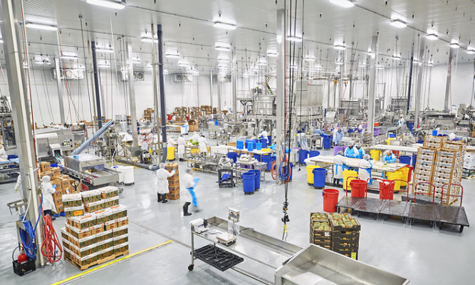
Cleanrooms are essential components of advanced manufacturing facilities, ensuring precise production of materials and technologies. From pharmaceutical manufacturing to aerospace manufacturing, and critical pieces of technology like semiconductor chips, cleanrooms have a significant role in ensuring the contamination-free production of these materials. Semiconductor chip manufacturing is a great example of a rapidly evolving and critical piece of technology that relies on the stringent operations at a much larger scale, with clean zones that range from modular cleanrooms to multiple level clean zones that can span up to several hundred thousand square feet.
Semiconductor chips are manufactured in facilities called fabrication plants (or fabs for short) and housed on massive campuses that span acres. The entirety of a fab is built to an exacting standard, and every detail, down to the choice of flooring systems, contributes to overall efficiency and performance.
Flooring systems specified for fabs, typically referred to as chemical resistant coatings, often go unnoticed but play a vital role in structural protection, contamination control, durability and the overall production efficiency of a fab. Developing chemical resistant coatings systems to meet rigors of a semiconductor fab ensures clean zones continue to support rapid innovation and production demands while minimizing maintenance downtime.
Why Semiconductor Cleanroom Flooring Matters More Than Ever
Semiconductor fabrication plants represent the most advanced manufacturing processes in the world, conducted in ultra-modern factories known for their stringent cleanliness requirements needed to transform silicon wafers to micro processing chips. Clean zones are critical to the fab’s overall operation and house cutting-edge equipment therefore unique and exacting design requirements must be taken into consideration.
The International Organization for Standardization (ISO) has established specific cleanroom classifications to suit various cleanliness needs under the ISO 14644–1 standard. These nine classification levels are based on the maximum number and size of particulates allowed per cubic meter, with a Class 1 designation being the cleanest.
Generally, the semiconductor and microelectronics industries demand the highest cleanliness, often due to the extreme sensitivity of the wafer area requirement of ISO 3 where wafers are exposed, whereas, in other areas of the fab, requirements may be ISO 4 or ISO 5. Clean zones, additionally, are constantly monitoring for Airborne Molecular Contamination (AMC) and therefore it is important to understand outgassing characteristics of coatings being specified.
Flooring plays a fundamental role in each of these clean environments and must meet rigorous standards to ensure chip quality and production equipment are not compromised. For example, modular cleanrooms within fabs frequently use static control flooring and often specify raised access floor panels to prevent any potential electrostatic discharge, which can lower the possibility of significantly damaging critical equipment like those in a semiconductor chip.
Addressing Chemical, Structural and Outgassing Challenges for Semiconductor Fab Clean Zones
Outgassing criteria for clean zones is a key consideration and must follow stringent standards laid out by the fab owner, which aid in controlling the levels of AMC from materials outgassing into the clean zone environment. Therefore, chemical resistant coating systems must be qualified by a manufacturer, tested by independent laboratories and approved by owners.
Chemicals such as solvents and acids are used in the wafer production process, which can corrode steel and concrete substrates within the facility. Any failure or degradation of the structural assets can lead to contamination of the clean zone air streams in the production area causing lost wafer batches and unexpected shutdowns.
Asset protection goes beyond the structure itself it also applies to the process and finished product. Chemical Resistant Coatings systems designed specifically for semiconductor fab environments will safeguard substrates from harsh corrosive chemicals and play a crucial role in ensuring continuous operations in Clean Fab and Clean Sub Fab Zones.
Structural Flooring Design for Semiconductor Fabs and Sub-Fabs
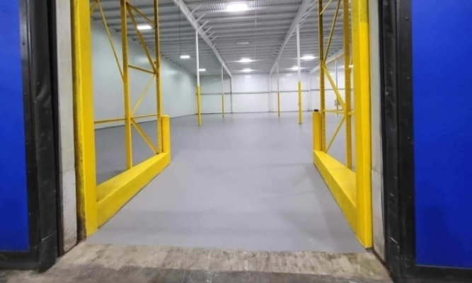
The structural design of a semiconductor clean zone is essential to its operational effectiveness, with flooring systems being a crucial component. A common design used in semiconductor fabs is the waffle slabs or cheese slabs depending on the needs of fab. This unique concrete slab design offers specific benefits that contribute to the overall structural integrity and operation of the fab.
The concrete waffle slabs and cheese slabs are made of reinforced concrete that provides excellent vibration control and a load-bearing capacity that is much greater than a traditional flat slab. Waffle slabs and cheese slabs also allow for utilities and communication lines to pass between the clean sub-fab – the area below a fab’s clean zone with specific systems that support the operation of all the equipment, while still supporting downdraft airflow crucial for contamination control.
Sustainable, Modular Semiconductor Cleanroom Flooring Systems
As the semiconductor industry evolves and chips become more significant in daily life, the demands on the fab and its clean zone flooring systems will also increase. While I can’t predict the future, my industry experience has provided me with several insights. Below are two semiconductor cleanroom flooring requirements that I believe will remain a priority in the future.
- Sustainability: With a growing emphasis on environmental impact and responsibility, semiconductor companies are paying special attention to their footprints and continually looking for ways to make their processes and production more sustainable and efficient. Sustainable and low-VOC materials will be crucial to the increased sustainability and decreased environmental impact of flooring systems.
- Modular Construction and Design: Offsite manufacturing is a growing trend within modern construction. This includes modular construction, which allows for faster timelines and reduced on-site labor. For cleanroom design, the flooring system is constructed onsite and must work along side other elements, such as the waffle/cheese slab, which can be fabricated offsite.
Chemical-Resistant Flooring Solutions That Support Long-Term Fab Performance and Innovation
When designing and building semiconductor fabs, every detail is important. Flooring systems play a significant role in contamination control, durability and shortened construction timelines. By understanding the unique requirements of cleanrooms and clean zones and using tailored high-performance flooring solutions, semiconductor fabs can continue to meet the growing demand for chips.
Designing effective flooring systems for cleanrooms and clean zones begins with having intimate knowledge of the semiconductor fab’s specific requirements before construction ever begins. The process of producing a semiconductor chip is an intricate one, and each fab is built with that fact in mind. The chemical-resistant coating systems in these unique clean environments must align with those same exacting standards.
As the industry progresses, flooring systems will need to adapt to new challenges and opportunities to ensure that cleanrooms remain effective for advanced manufacturing. Whether through sustainable materials or modular designs, future flooring systems will be crucial in supporting semiconductor fabs and the vital technology they enable.
Partner with Sherwin-Williams for Proven Semiconductor Cleanroom Flooring Solution
From chemical-resistant coatings to sustainable, modular systems, Sherwin-Williams delivers the expertise and technology needed to meet the demanding standards of today’s semiconductor fabs. Our semiconductor manufacturing flooring solutions are engineered to help protect clean zones, support continuous operation and prepare facilities for the next generation of chip production.
Contact us today to learn how Sherwin-Williams can help you design and specify flooring systems that enhance performance, reduce downtime and ensure long-term reliability across your semiconductor fabrication facilities.
Discover More
Industry Expertise and Innovation
See how we help customers find customized solutions for their project and application challenges.

Industry Solutions
Explore technology and innovation to protect your most valuable assets.
LEARN MOREProduct Lookup
Find out more about our innovative coatings for a variety of industries.
FIND A PRODUCT